AMD CEO Lisa Su became CEO in October 2014, but she started working for the company a little earlier & ; in January 2012. By that time, current CTO Mark Papermaster had already begun to form a development team to offer a new approach to processor design, creating the Zen architecture. The participants of the event shared their memories in the pages of IEEE Micro.
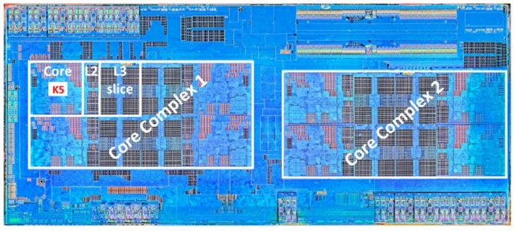
Throughout 2012, the team of specialists created by Papermaster was trying to find ways to eliminate the lag in the rate of processor performance increase, which AMD suffered from in those years not only in the desktop, but also in the server segment of the market. There was no point in developing the Bulldozer architecture further, because this branch of AMD processor evolution turned out to be a dead end. It was Mark Papermaster, in those years, invited Jim Keller, who had already had a hand in creating K7 and K8 processor architectures, to work at AMD, but then he left the company. Under Jim's leadership AMD development teams were restructured: experts in high-performance and low-cost architectures were united in one team. They were tasked with creating a new scalable modular architecture that could be used effectively in both mobile and desktop or server segments. Developers had to catch up and provide 40 % increase of specific performance in comparison with the previous AMD architecture. It was Mike Clark, who participated in the development of the first generation Zen architecture, that gave it a name, based on a balance of necessary qualities in terms of performance, power consumption and transistor density. In addition, a team of experts was tasked with monitoring the energy efficiency of AMD projects. The result is a 52% increase in performance, surpassing the initial target. AMD gave up on K12 processor development with ARMv8 architecture for server-based applications at that time, but the freed up human resources were used for Zen 3 architecture development. In fact, this work was implemented in parallel with the development of Zen 2 architecture & ; the latter was developed by the same experts, as Zen of the first generation. It turns out that the architecture Zen 3 was largely created from scratch, but between Zen, Zen + and Zen 2 there was obvious continuity. A modular approach to processor design using a high-speed Infinity Fabric interface for data exchange between individual blocks allowed AMD to easily master multi-chip layout using heterogeneous chipsets. Processors used in both notebooks and supercomputers have been created on common basic blocks, and development time for new models has been greatly reduced. To illustrate this, the authors of the article showed an image of a 14nm Zen processor chip, overlaid with the outline of a hypothetical K5 processor in the dimensions it would have had if it had been released on 14nm technology. An 8-core Zen processor would be about the size of 400 such K5 generation processors. While that generation processor contained only 4.3 million transistors, the representative of the Zen generation increased it to 4.8 billion.