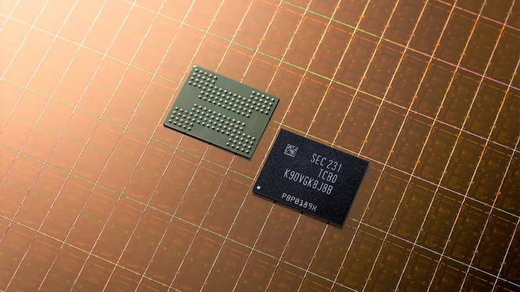
Samsung has announced the start of mass production of 3D V-NAND TLC flash memory chips of new, 8th generation, writes Tom's Hardware portal.The new chips have a capacity of 1 Tbit (128 GB) and presumably consist of 236 layers, although Samsung does not specify this aspect.The manufacturer only calls the novelty flash memory with the highest bit density in the industry.Image source: SamsungFlash memory chips Samsung 3D V-NAND TLC 8th generation can provide transfer speeds of 2400 MT / s and in combination with advanced controllers can be used in the consumer solid-state drives with PCIe 5.0 interface.According to Samsung, such SSDs will offer data transfer rates in excess of 12.4 Gbytes/sec.Samsung claims that the use of new manufacturing technology has made it possible to get more memory from a single silicon wafer - an increase of 20 percent compared with previously produced flash memory chips of the same capacity.This will ultimately result in lower manufacturing costs, and could potentially mean cheaper SSDs for consumers.Details on the architecture of the new 8th generation 3D V-NAND TLC chip have not been disclosed by the company.According to Tom's Hardware, like other manufacturers, Sasmung gets memory with more than 200 layers by stacking 128-layer crystals on top of each other.During the \"lapping\" process some of the layers get lost, which does not allow for the ideal of a 256-layer 3D NAND chip, but nobody stops you from striving for it.So earlier this year, Micron introduced 3D NAND chips with 232 layers, and SK hynix - with 238 layers.About the first products based on the new flash memory chips Samsung also does not say anything yet.